|
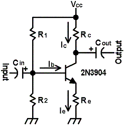
Common-Emitter Amplifier
The Common-Emitter (CE) amplifier is the most common type of amplifier configuration used in analog and digital circuits. It provides:
- Modest voltage gain (AV).
- High input impedance (few KΩ).
- Inverted output (180º phase shift).
Symbols and Terms
Av: Voltage gain, the ratio of the output voltage to the input voltage.
Beta (Β): DC current gain, the ratio of the collector current to the base current.
Cutoff: Collector current reduced to zero.
Q-Point: Quiescent or resting values of collector current (Icq) and voltage (Vceq) with no input signal applied.
Ib: Base current.
Ic: Collector current.
Ie: Emitter current.
Vce: Voltage between the collector and emitter.
Vbe: Voltage between the base and emitter.
The output current of a transistor is a function of the input current and the transistor Beta ( Ic = Ib * Beta ). Technically, Ie is the sum of Ib and Ic. Because Ib is so small relative to Ic, it is often eliminated from any calculations involving Ie ( Ie ~ Ic ). This simplifies some of the equations.
Most amplifiers need to work with input signals having both positive and negative voltage swings. To accomplish this, the amplifier is designed in a Class A configuration, the collector current is offset from zero without an input signal present. This is easily accomplished by biasing the base current, using R1 and R2.
The collector resitor (Rc) develops the ouput voltage, based on changes in the collector current responding to the input signal. The emitter resistor (Re) ensures the collector voltage can make large swings without trying to exceed (Vcc) or drop to ground (0VDC).
The input capacitor (Cin) and output capacitor (Cout) provide an AC-coupled design. The capacitors block any DC current that might upset the bias of the transistor.
Designing the Amplifier (Do the math)
- Choose the basic operating parameters:
- Vcc = 12 VDC, the power supply voltage.
- Av = 5, a medium value of gain for this typoe of amplifier.
- Icq = 4mA, keeping power dissipation low.
- Vceq = 5 VDC, about one-half of Vcc.
- Beta = 150, based on the specifications of the transistor.
- Vbe = 0.7 VDC, typical for a silicon transistor.
- Calculate the values of Rc and Re:
- Vcc = (Ic * Rc ) + Vceq + ( Ie * Re ) -- and since Ic ~ Ie
- Vcc = (Ic * Rc ) + Vceq + ( Ic * Re ) -- so
- ( Vcc - Vceq ) / Ic = Rc + Re = Vceq + Ic * ( Rc + Re ) -- so
- Rc + Re = ( 12 V - 5 V ) / 4 mA = 1.75 kΩ -- or
- Re = 1.75 kΩ - Rc
- Calculating Vin:
- Vin = Vbe + Ic * Rc -- assuming a silcon junction (Vbe 0.7 )
- Vin = 0.7 + Ic * Rc ~ Ic * Rc
- Calculating Vout:
- Vout = Vcc - Vceq - Ic * Re -- substituting Vcc with
- Vcc = Ic * Rc + Vceq + Ic * Re -- results in
- Vout = Ic * Rc + Vceq + Ic * Re - Vceq - Ic * Re = Ic / Rc
- Continuing:
- Av = Vout / Vin = Ic * Rc / Ic * Re = Rc * Re
- Av = 5 = Rc / Re -- therefore
- Rc = 5 * Re = 5* (1,750 Ω - Rc) = 8,750 Ω - (5 * Rc ) -- simplifies to
- ( 6 * Rc ) = 8750 Ω -- resulting in
- Rc = 1,458 Ω
-- selecting 1.5 kΩ as a standard value.
- Re = 1,750 Ω - Rc = 1,750 Ω - 1,458 Ω = 292 Ω
-- selecting 270 Ω as a standard value.
- Establish Ib:
- Ib = Icq / Beta = 4 mA / 150 = 26.7 µA
- Establish the current through R1 and R2 as equal to 10 times Ib as a rule of thumb.
- IR1R2 = 10 * 26.7 µA = 270 µA
- Calculate R1 and R2:
- VR2 = Vbe + Ic * Re = 0.7 V + ( 4 mA * 270 Ω ) = 1.78 V
- R2 = VR2 / IR1 = 1.8 V / 27 µ:A = 1.8 V / 0.000270 A = 6,666 Ω
-- selecting 6.8 kΩ as a standard value.
- VR1 = Vcc - 1.8 V = 12 V - 1.8 V = 10.2 V
- R1 = VR1 / IR1 = 10.2 V / 27 µA = 10.2 V / 0.000270 A = 37,777 Ω
-- selecting 37.8 kΩ as a standard value.
Based on Hands-On Radio from Feb-2003 QST
|